
A materials challenge moves to the centre of chip design
Intel and China-based Lens Technology announced their collaboration on 24 July 2026, positioning precision glass processing as a potential building block for future semiconductor packages. The agreement is exploratory rather than a product launch: the companies said they will examine ways to speed development and eventual scaling of packaging based on glass substrates.
That distinction matters. No commercial processor, manufacturing volume, customer programme or deployment date was announced. Yet the partnership is significant because it addresses a constraint that is becoming more visible as AI accelerators, high-bandwidth memory and specialised compute components are assembled into ever-larger multi-die packages.
Advanced packaging increasingly determines how much compute, memory and high-speed connectivity can be combined in a practical system. Instead of relying solely on one huge piece of silicon, chipmakers can join several chiplets and memory stacks in a single package. The approach can improve design flexibility and yield, but it sharply raises demands on the substrate beneath those components: it must route far more signals, deliver power efficiently, remain flat through processing and operation, and manage mechanical stresses across a large area.
Why glass is attracting attention
Most high-end packages still use organic substrates. These materials are established, manufacturable and economically important, but their dimensional behaviour becomes more difficult to control as package sizes and connection densities rise. Heat and mechanical stress can cause warpage, complicating lithography, assembly, thermal contact and long-term reliability.
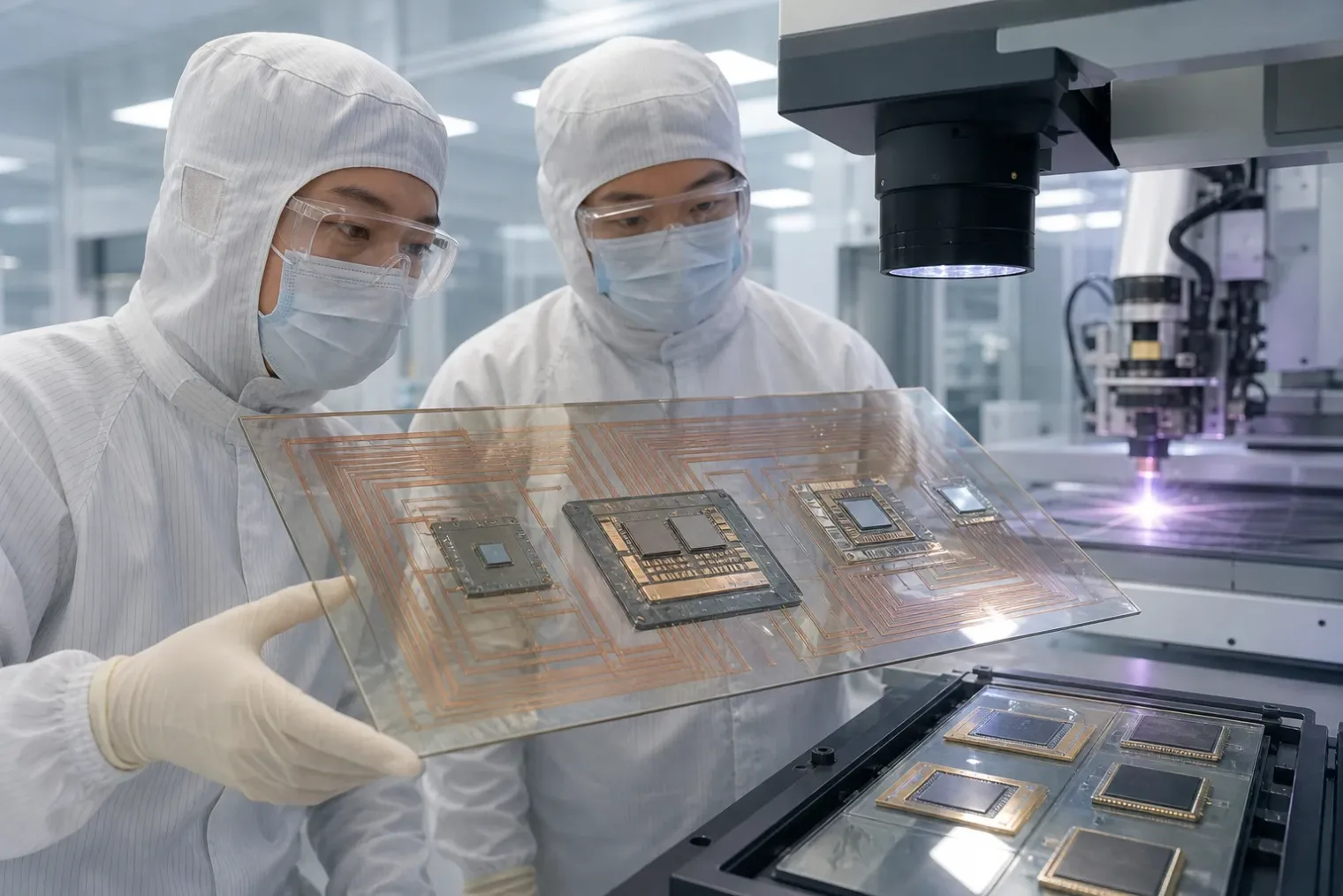
Glass offers a different combination of properties. Its flatness, rigidity and dimensional stability can support finer routing features and more precise alignment between layers. Its thermal expansion can also be tailored closer to that of silicon than many organic alternatives, helping to reduce stress caused when materials expand and contract at different rates.
For high-speed electrical links, glass is also attractive because it can have lower signal loss than silicon at relevant frequencies. Through-glass vias, which are vertical electrical connections formed through a glass core, could add another path to higher connection density. Glass can moreover be produced in large panel formats, a potential advantage for large package substrates if manufacturing yields can be maintained.
Intel has been developing glass-substrate technology for more than a decade. In 2023, it said its research indicated that glass could enable an order-of-magnitude increase in interconnect density relative to contemporary organic substrates, as well as larger package formats and higher-temperature processing options. These are technology targets and material-level advantages, not a guarantee that every future glass-based package will deliver the same gains.
The collaboration brings together complementary capabilities. Intel contributes chip architecture and advanced-packaging development, while Lens Technology brings expertise in precision glass materials, laser processing and high-volume manufacturing. The practical importance of that combination is clear: a promising substrate material is useful only if manufacturers can shape it, drill and metallise vias, build multilayer routing on it, inspect defects and handle it at scale with acceptable yield.
AI workloads make packaging a system issue
The immediate commercial logic is centred on AI and data-centre hardware. These systems require large amounts of bandwidth between compute dies and memory, while their electrical and thermal budgets are increasingly restrictive. A packaging substrate does not create transistor performance by itself, but it can determine whether the surrounding system can use that performance effectively.
Higher-density interconnects could allow designers to place more chiplets within a given package area or to connect them with shorter, more direct paths. Better dimensional stability may help manufacturers produce larger multi-die assemblies with fewer alignment-related problems. Improved power-delivery routing and lower-loss signalling could be especially valuable as data rates rise.
Intel and Lens Technology also identified AI PCs, server thermal and structural components, robotics, industrial equipment and edge computing as possible future areas of cooperation. These possibilities should be read as a broad technology agenda rather than a confirmed product roadmap. The near-term focus remains the harder task of making glass-substrate packaging manufacturable for advanced computing.
The engineering hurdles remain substantial
Glass is not a simple replacement for organic packaging materials. It is inherently susceptible to crack formation, and thin, large-area panels can be difficult to handle. The via-formation process is particularly important: local stress around through-glass vias, metal-filled structures and interfaces can create failure risks during processing or thermal cycling.
Research on glass packaging repeatedly identifies microcracks, stress at via edges, delamination and thermal-expansion mismatch as central reliability concerns. The necessary mitigations extend beyond the glass composition itself. Via geometry, surface preparation, laser or etching methods, metallisation, build-up layers, panel handling and package-level design all affect the final result.
This is why production expertise has strategic value. An advanced substrate must not only demonstrate electrical performance in a laboratory; it must survive repeated manufacturing steps and meet reliability requirements at viable cost. The industry will also need supporting equipment, materials, inspection methods and qualification standards to mature alongside the substrate.
A long-term packaging bet, not an immediate platform shift
Intel previously indicated that complete glass-substrate solutions were targeted for the latter half of the 2020s. The new partnership does not revise that timetable, but it suggests that the company sees external manufacturing collaboration as important to turning its research into a scalable packaging option.
For Lens Technology, the deal opens a route from precision glass processing in established technology markets towards semiconductor supply chains, where qualification cycles are long and reliability thresholds are high. For Intel, it could add specialist materials and processing capacity to an effort that must reach beyond conventional chip fabrication.
The larger implication is that performance progress in AI hardware will increasingly depend on materials and assembly technologies that sit outside the transistor itself. Glass substrates are unlikely to displace organic packaging everywhere soon; established materials will remain appropriate for many products. But in the largest, fastest and most densely integrated systems, glass could become an important option if its manufacturability and reliability challenges are solved.
Intel and Lens Technology have therefore announced an early-stage industrial partnership around a credible technical direction. Its eventual importance will be measured not by the announcement, but by whether glass cores can move from demonstrations and qualification programmes into dependable, high-volume AI and data-centre packages.
Sources
- Intel and Lens Technology Collaborate to Enable Advanced Semiconductor Packaging for the AI Era — Intel Newsroom
- Intel Unveils Industry-Leading Glass Substrates to Meet Demand for More Powerful Compute — Intel Newsroom
- Glass Core Substrate — IEEE Electronics Packaging Society
- Process Integration and Reliability Challenges of Through-Glass Vias for Glass-Based Advanced Packaging: A Focused Review — PubMed Central
- Intel Advanced Packaging for Bigger AI Chips — IEEE Spectrum


