
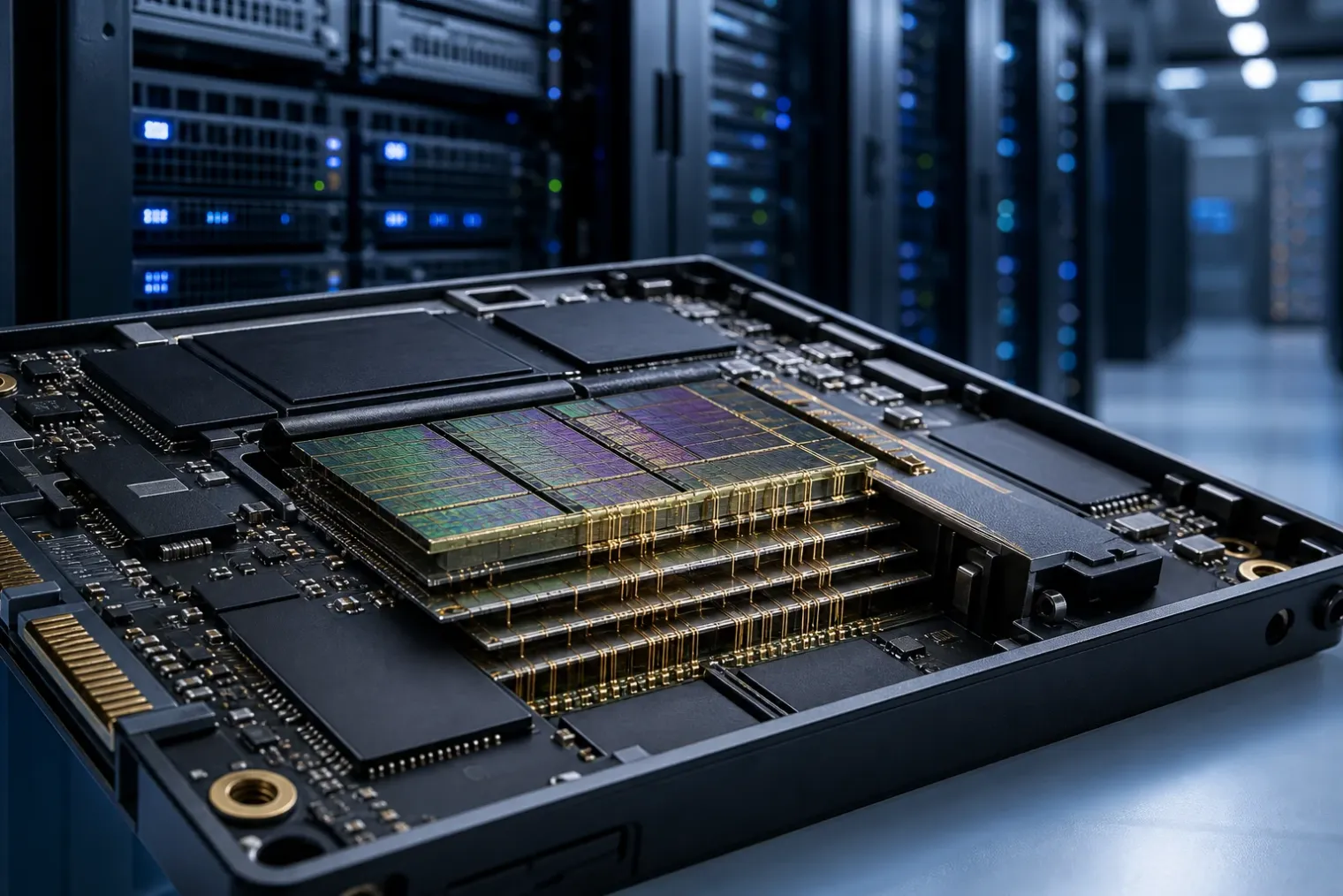
A density-focused advance in 3D NAND
Kioxia and Sandisk have unveiled a new high-performance Quad-Level Cell, or QLC, 3D flash technology built on their tenth-generation BiCS architecture. The companies presented the development at the Future of Memory and Storage conference in Santa Clara, California, on 4 August 2026, positioning it for infrastructure that needs very large solid-state storage pools rather than for immediate retail SSD launches.
The central claim is density. Kioxia says the 2Tb QLC device reaches 37.6Gb per square millimetre, a figure it describes as the highest achieved among QLC products. The new chip uses 332 stacked word lines, a considerable increase in vertical complexity, alongside a six-plane layout intended to raise parallelism within the die. Together, those changes address a core NAND challenge: fitting more data into a small silicon area without allowing write speed or energy use to deteriorate too sharply.
QLC stores four bits in each cell, compared with three bits in TLC flash. That makes it attractive for capacity-led SSDs because more information can be held in the same physical space. The compromise is that distinguishing among more charge states is more difficult, which can constrain endurance and write behaviour. The importance of the new announcement therefore lies not only in the density figure, but also in the engineering intended to narrow those operational trade-offs.
Architecture is doing more of the scaling work
The device continues the partners’ use of CMOS directly Bonded to Array, or CBA, manufacturing. In this approach, the memory-cell array and the CMOS circuitry are manufactured separately and then bonded together. That can enable each section to be optimised independently, avoiding some of the layout constraints of designs in which peripheral circuitry occupies space alongside the array.
For the QLC product, Kioxia has adopted a 1×6 floor plan rather than a 2×3 arrangement. The change is designed to reduce bonding-pad area and shrink the overall die footprint. It also introduces engineering difficulties, including power-delivery resistance, electrical noise and interference between planes operating asynchronously. Kioxia says it addressed these issues with additional power wiring, revised ground-pad placement and dedicated quiet ground connections for noise-sensitive circuits.
A six-plane design matters because planes are semi-independent regions of a NAND die that can be accessed in parallel. More planes can improve concurrency, helping a high-capacity chip sustain usable performance when integrated into large SSD arrays. The companies are therefore treating density as a system-level issue, not simply a matter of adding more layers.
Write speed and idle power remain QLC’s practical tests
Kioxia reports write throughput above 85MB/s for the chip. It attributes part of the improvement to a new sensing method called Local BUS Coupling Sense. Programming QLC is inherently more demanding than programming TLC because the device must place cells accurately into a greater number of charge states. The new technique shortens part of the verify process by allowing operations that would normally be sequential to proceed in parallel. Kioxia says this raises write throughput by 4.2% relative to its conventional technique.
The companies have also developed a power-saving capability called Bus Idle Sleep. In high-stack packages, multiple flash dies may remain powered while a different die is carrying out data input or output. Kioxia says the approach automatically places unselected dies into an internal standby state, cutting their idle current from tens of milliamps to hundreds of microamps. That reduction becomes more meaningful as packages contain more dies and data-centre storage density rises.
The announced QLC technology also uses an interface rated at up to 4.8Gb/s. This follows the tenth-generation TLC device that Sandisk began sampling in July, which introduced the same 332-layer generation and a 4.8Gb/s interface. The QLC version applies that platform to a different objective: maximising usable capacity while retaining enough bandwidth for enterprise deployments.
Manufacturing makes the announcement more consequential
This is not an isolated laboratory result. Kioxia and Sandisk began production of tenth-generation 3D flash products at Fab2 at the Kitakami Plant in Iwate Prefecture, Japan, on 3 July 2026. The facility had previously produced eighth-generation products and is being scaled for the newer technology. That production milestone gives the QLC announcement a more credible path towards commercial drives, although the companies have not specified product availability, SSD capacities or customer qualification schedules for this particular chip.
Their manufacturing relationship is also long term. In January, the companies extended their joint-venture arrangements at the Yokkaichi and Kitakami plants through 31 December 2034. This shared development and production model gives both businesses scale in a market where investment requirements for advanced NAND fabrication are substantial.
The likely destination is high-capacity enterprise storage
The near-term use case is likely to be data-centre SSDs designed to increase storage per server and per rack. AI deployments, analytics systems, content repositories and cloud platforms create demand for large flash pools, but operators also closely measure power consumption, physical density and serviceability. A denser QLC die can reduce the number of packages needed for a given SSD capacity, potentially helping with all three measures.
It would be premature, however, to treat the technology as a direct signal of imminent consumer-drive upgrades. Kioxia and Sandisk have framed the development around next-generation infrastructure, and the reliability, firmware and controller decisions made by SSD makers will determine how its capability translates into end products. The announcement is better understood as a building block: a QLC NAND platform that attempts to push density forward while preserving the bandwidth and energy characteristics needed for large-scale storage systems.
Sources
- Kioxia and Sandisk Unveil New High-Performance QLC 3D Flash Memory — TechPowerUp
- Development of a 10th Generation 2Tb 4b/cell BiCS FLASH product — Kioxia
- Kioxia and Sandisk Begin Production of 10th-Generation 3D Flash Memory Products at Kitakami Plant Fab2 — Kioxia
- Sandisk Announces Sampling of BiCS10 1Tb TLC 3D NAND Flash Memory — Sandisk
- Kioxia and Sandisk demonstrate the world's highest-density 3D NAND flash — Tom's Hardware


