
A project whose price tag has changed
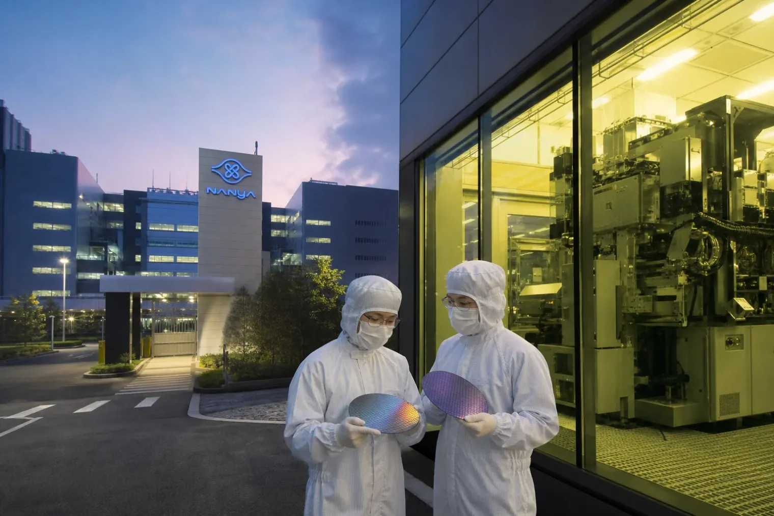
Nanya Technology’s planned Fab 5A in New Taipei City is often described as a US$10.7 billion investment in 10nm-class DRAM and extreme-ultraviolet lithography. That figure reflects the company’s original announcement in April 2021, when it outlined an approximately NT$300 billion, three-phase project.
The latest disclosed plan is larger. In its results for the second quarter of 2026, Nanya said total planned capital expenditure for the fab’s eventual full capacity was estimated at NT$480 billion. Using recent exchange-rate ranges, that is materially above the earlier US-dollar estimate. The US$10.7 billion headline is therefore best understood as the earlier framing of a project that has since expanded in nominal local-currency terms and been rescheduled.
The programme remains strategically important because it combines a substantial increase in wafer capacity with a transition to more advanced DRAM manufacturing. Nanya is one of Taiwan’s established DRAM producers, but it competes in a market dominated by much larger suppliers including Samsung Electronics, SK hynix and Micron Technology. Fab 5A is intended to give the company greater scale while supporting a broader mix of server, mobile, industrial and AI-related memory products.
Capacity starts in 2028
Nanya now expects the first phase of the new fab to reach 30,000 wafer starts per month in 2028. The full plan targets 45,000 wafer starts per month. A wafer start measures material entering the manufacturing process rather than finished memory chips, so the eventual output will depend on chip design, die size, yields and product mix.
The schedule is later than the timeline presented in 2021. At that point, Nanya had envisaged completing construction in 2023 and beginning volume production in 2024. By April 2026, the company said equipment installation was planned for the first quarter of 2027. The more recent target for first-phase capacity in 2028 illustrates the long lead time involved in building, equipping and qualifying a sophisticated memory fab.
This matters for the market as well as for Nanya. New DRAM capacity cannot respond immediately to a price surge: construction, tool installation, process development and customer qualification can take years. As a result, even a large investment announcement should not be read as near-term relief for tight memory supply.
EUV is a technology commitment, not a product claim
Fab 5A is designed for 10nm-class DRAM technology and EUV lithography. In DRAM, the “10nm-class” description is an industry naming convention rather than a direct statement that every physical feature measures 10 nanometres. Nanya has referred to a progression of nodes including 1C, 1D and 1E, with EUV capabilities developing alongside them.
EUV uses very short-wavelength light to print increasingly intricate patterns on silicon wafers. Its adoption can reduce patterning complexity at selected layers, but it also raises the capital intensity and operational demands of production. The value of EUV to Nanya will depend not simply on installing the equipment, but on achieving repeatable yields, acceptable throughput and commercially competitive cost per bit.
That distinction is significant. A new node or lithography capability does not automatically translate into leadership products. Nanya must convert its process work into qualified DRAM devices that meet customer requirements for performance, power consumption, reliability and supply continuity. Its current portfolio spans DDR5, LPDDR5/5X and legacy generations, while the company has also highlighted customised memory and AI infrastructure products as areas for higher-value growth.
A favourable market supports the spending case
The decision to extend the fab plan comes during an exceptional upturn in memory pricing. Nanya reported second-quarter 2026 revenue of NT$82.55 billion, up 68.2% from the preceding quarter. Its gross margin reached 79.5%, while net income was NT$50.19 billion. Average selling prices increased by more than 60% quarter on quarter, whereas bit shipments were flat.
Those figures show that pricing, rather than an immediate volume expansion, was the central driver of the quarter’s improvement. In the first half of 2026, Nanya said AI infrastructure and server applications accounted for more than 20% of revenue. Its April private placement, subscribed by four major customers, was also intended to reinforce supply relationships.
Industry forecasts point to a broader supply-demand imbalance. Gartner projected that DRAM prices would rise 125% in 2026, driven by AI infrastructure investment and constrained availability, although it also warned that elevated memory costs could suppress non-AI demand and that meaningful price relief might not arrive until late 2027.
For Nanya, strong pricing and customer interest create a more supportive financial setting for long-duration capital expenditure. However, memory markets are cyclical. A fab built for demand conditions in 2028 and beyond must remain economically viable if prices normalise, customers change product plans or rival producers add supply faster than expected.
Execution will determine the strategic result
Fab 5A should be viewed less as a single announcement than as a multi-year reset of Nanya’s manufacturing base. The original project established the ambition; the NT$480 billion estimate reflects the higher cost and expanded scope now associated with delivering it. The first 30,000-wafer phase is planned for 2028, with the remaining capacity to follow.
The investment could improve Nanya’s ability to serve growing demand for conventional and low-power DRAM, particularly where customers value supply diversity. It may also create a platform for more advanced and specialised products. Yet the project faces the familiar risks of semiconductor manufacturing: construction delays, equipment availability, process complexity, yield learning and the possibility that today’s unusually high prices will not persist.
The immediate conclusion is therefore measured. Nanya is committing to a much larger and more technologically demanding fab programme than the US$10.7 billion description suggests. Its success will be judged not by the announced expenditure alone, but by whether Fab 5A reaches its 2028 capacity target and delivers competitive DRAM at scale.
Sources
- Nanya Announces $10.7B Investment in Fab5A, Aims for 10 nm-Class EUV DRAM — TechPowerUp
- Nanya Technology to Invest an Advanced DRAM FAB in New Taipei City — Nanya Technology
- Nanya Technology Reports Results for the Second Quarter 2026 — MarketScreener / Publicnow
- Gartner Forecasts Worldwide Semiconductor Revenue to Exceed $1.3 Trillion in 2026 — Gartner


