
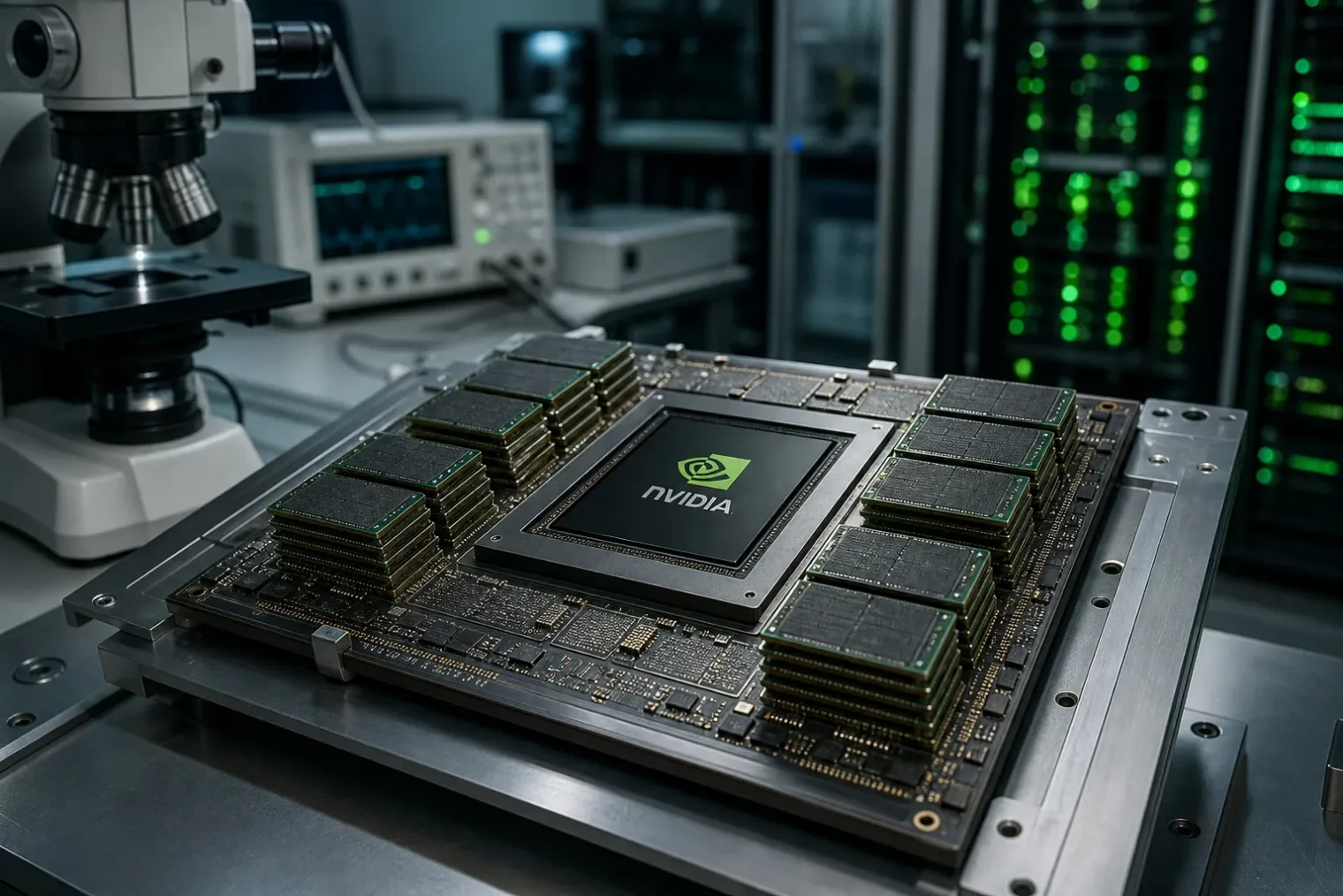
A new role for high-bandwidth memory
NVIDIA has introduced NVHBM as a custom high-bandwidth-memory implementation for partners building their own AI accelerators, rather than as a standalone memory standard for the wider market. The technology is part of NVIDIA’s NVLink Fusion programme, which lets customers combine custom CPUs and accelerators with NVIDIA’s rack-scale connectivity and system architecture.
The central claim is significant: NVHBM can provide up to 30% more memory bandwidth per stack than standard HBM4E, while reducing HBM power use by up to 15%. NVIDIA also says the design can free up to 25% more area on an accelerator’s compute die. These figures are company projections based on a particular architecture, not independently published product benchmarks, but they address constraints that increasingly shape AI-chip design.
For large language models and other generative-AI workloads, arithmetic throughput alone is not enough. Accelerators must repeatedly load model weights, activations and inference-state data, including key-value cache contents. If those data transfers cannot keep pace with the compute engines, expensive matrix units sit idle. This makes memory bandwidth, package area, power delivery and cooling interdependent design problems.
Moving the controller into the memory stack
Conventional HBM implementations place substantial memory-interface circuitry on the processor or accelerator die. NVIDIA’s approach instead puts its custom memory controller into the HBM base die, the logic layer beneath the vertically stacked DRAM dies. It also uses a custom physical interface, or PHY, between the accelerator and the memory stack.
That rearrangement is intended to reduce the area and routing burden imposed by the memory interface. NVIDIA says its PHY and supporting area can be reduced by as much as 67% compared with a standard HBM4E implementation. The narrower interface can simplify routing on the interposer, the advanced package layer that electrically connects the compute die and multiple memory stacks.
The practical attraction is not merely a smaller interface. Within a fixed package size, silicon recovered from memory-interface functions can be reassigned to compute blocks, cache, networking logic or accelerator features tailored to a cloud provider’s own workloads. NVIDIA describes as much as a 30% increase in available main-die silicon in some layouts, while presenting the broader XPU benefit as up to 25% more compute-die area.
Those distinctions matter. Area released by a physical layout does not automatically translate into a proportional gain in end-user performance. A chip designer must decide how much of that space becomes additional compute, local memory, specialised processing or power-management circuitry. The workload, software and the balance of the full system will determine whether the reclaimed area produces a material improvement.
Bandwidth is valuable, but not universal
A 30% increase in bandwidth per HBM stack could be especially important for memory-bound inference and training stages. Faster access to weights and cached context can improve accelerator utilisation and raise the number of tokens served per device when memory traffic is the limiting factor. It may also allow designers to pursue similar throughput with fewer memory stacks, although capacity requirements will often prevent that trade-off.
The gain should not be read as a blanket 30% improvement for every AI task. Compute-bound operations may see little direct benefit from additional off-chip bandwidth. In distributed training and inference, bottlenecks can also arise in the interconnect between accelerators, storage pipelines, software scheduling or power limits. NVIDIA itself presents NVHBM as one component of a co-designed system rather than a replacement for rack-scale networking.
The company says the combined effects of higher memory bandwidth, added die area and lower HBM power could yield up to a 30% end-to-end performance increase per custom XPU. That outcome depends on how a partner uses the area and power headroom, and on whether its applications are constrained by memory movement. It is best understood as an architectural target rather than a guaranteed uplift for every deployment.
Lower memory power has system-level implications
HBM energy consumption is a growing concern because its effects extend well beyond the memory stacks. Lower memory power can reduce heat within the package, ease cooling demands at the server level and create headroom within a rack’s power envelope. NVIDIA estimates NVHBM can cut HBM power consumption by up to 15% relative to standard HBM4E.
At hyperscale, even incremental efficiency changes can affect how many accelerators a facility can operate within its available electrical and cooling capacity. NVIDIA argues that the savings could be substantial across very large installations. The actual benefit, however, will depend on the share of total accelerator power consumed by HBM, which varies by chip, workload and operating point.
The larger strategic point is that custom AI silicon is no longer designed in isolation. Memory architecture can determine how much compute fits within a package and how much useful work a rack can sustain under thermal and electrical limits. NVHBM is an attempt to turn that packaging constraint into a differentiator for NVIDIA’s platform partners.
A route into custom AI chips
NVHBM is tied to NVLink Fusion, NVIDIA’s effort to make its scale-up technology available to makers of semi-custom AI infrastructure. The model allows a hyperscaler or AI-focused company to develop an XPU or CPU while using NVIDIA components and system building blocks for high-speed connectivity, switching, rack integration and software.
NVIDIA says NVHBM will be validated with multiple memory suppliers, which could lower the work required to qualify memory across suppliers. The company has also identified Amazon’s Annapurna Labs as the first collaborator on the technology. Amazon has said the work will extend its NVLink Fusion relationship and support future Trainium infrastructure.
This positioning is notable because it expands NVIDIA’s role beyond selling finished GPUs. The company is offering key intellectual property around packaging, memory and interconnects to customers that may also be designing alternative accelerators. For those customers, the appeal is access to an established scale-up ecosystem. For NVIDIA, it is a way to keep custom silicon connected to its broader infrastructure stack.
What remains to be demonstrated
NVHBM arrives before public, independently measured products based on the design. Important details remain undisclosed, including bandwidth in absolute terms, capacity options, data rates, latency characteristics, compatibility boundaries and the timeline for production systems. It is also unclear how broadly the implementation will be adopted among memory manufacturers and accelerator developers.
Still, the announcement highlights where competition in AI hardware is moving. The next gains will not come only from more transistors or faster compute engines. They will increasingly come from advanced packaging and from tighter co-design among logic, memory, interconnect, power and software.
NVIDIA’s NVHBM proposal reflects that shift. Its promised bandwidth and efficiency gains are compelling for memory-limited AI workloads, but their commercial importance will rest on the first partner chips, the availability of qualified memory and measured performance in real data-centre deployments.
Sources
- NVIDIA NVLink Fusion Brings NVHBM to Next-Generation AI Infrastructure — NVIDIA Technical Blog
- NVIDIA NVLink Fusion Expands With NVHBM Custom High-Bandwidth Memory — NVIDIA Blog
- AWS and NVIDIA to Deliver 2 Million Additional GPUs and Next-Generation Infrastructure for Agentic and Physical AI — NVIDIA Newsroom


