
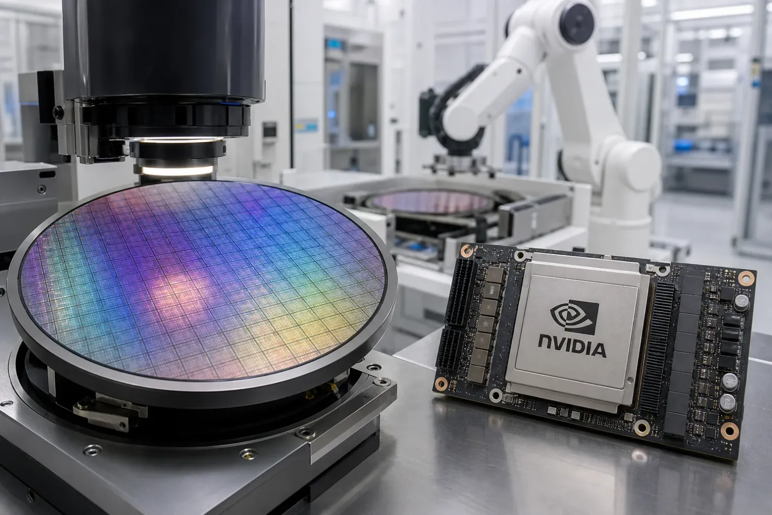
A reported supply agreement, not a confirmed product specification
Nvidia has reportedly secured access to TSMC’s A16 manufacturing process for GPUs based on its future Feynman architecture. The report is significant because it places Nvidia near the front of the queue for a process designed specifically to address the routing and power-delivery constraints of high-performance computing chips.
The wording matters, however. Neither Nvidia nor TSMC has publicly confirmed a customer-specific A16 supply agreement, the size of any reservation, or the exact Feynman dies that would use the technology. The available reporting should therefore be read as an account of supply-chain planning rather than as a final product announcement.
Nvidia has publicly placed Feynman after the current Vera Rubin generation and its successor in its multi-year data-centre roadmap. The company’s presentations have associated Feynman with 2028, but have disclosed comparatively few architectural details. A process-node decision, even if accurately reported, does not establish performance, product timing, configurations or whether every part of a broader platform will be made on the same process.
Why A16 is relevant to AI accelerators
TSMC introduced A16 as an extension of its N2 family rather than as a conventional, clean-sheet node transition. Its distinguishing feature is Super Power Rail, a backside power-delivery approach paired with nanosheet transistors. Moving power-routing elements to the back of the silicon is intended to free routing resources on the front side for signals.
That design target is particularly relevant to large AI and high-performance computing processors. Such chips must distribute substantial power across dense arrays of compute units while also carrying high-speed signals for memory, chip-to-chip communication and I/O. At advanced geometries, power and signal routing can become as important a constraint as transistor density.
TSMC has said A16 is best suited to high-performance computing products with complex signal routes and dense power-delivery networks. Against its N2P technology, the foundry has projected an 8% to 10% speed improvement at the same power, a 15% to 20% power reduction at the same speed, and up to a 10% density gain for data-centre products. These are process-level targets, not promised improvements for a particular Nvidia processor. The eventual outcome will depend on Nvidia’s architecture, libraries, physical design, clock targets and packaging choices.
The principal attraction, then, is not simply a smaller marketing label. For a large accelerator operating within a power-constrained rack, gains in voltage delivery and usable routing headroom could help Nvidia pursue higher throughput or better efficiency without relying solely on a larger die.
Capacity and execution are the real constraints
TSMC’s public schedule gives the report a plausible industrial context. The company has stated that A16 volume production is scheduled for the second half of 2026. Yet the beginning of volume production at a foundry is not the same as broad availability of mature, high-yield capacity for the largest and most demanding chips. Early production is usually allocated cautiously, and the most advanced customers may need to commit to capacity well ahead of their own launches.
For Nvidia, securing leading-edge wafers would be only one part of the task. Modern AI systems require several constrained components and services at once:
- advanced logic wafers for compute and supporting dies;
- high-bandwidth memory and its associated base dies;
- advanced packaging to connect large numbers of components;
- substrates, interconnects, networking silicon and system-level thermal hardware.
This is why a future Feynman platform is unlikely to be defined by A16 alone. Nvidia’s current Vera Rubin platforms already combine GPUs, CPUs, networking and other silicon into rack-scale systems. As platforms expand, the ability to assemble a balanced system at volume can matter more than access to an individual manufacturing node.
It also explains reports that Nvidia could use a mix of process technologies across a multi-die design. Using A16 only where its power-delivery and performance characteristics add the greatest value, while making less critical dies on a more established node, would reduce pressure on scarce leading-edge capacity. Such an approach would be consistent with the wider industry move towards heterogeneous packaging, though Nvidia has not confirmed a Feynman die strategy.
Strategic implications for Nvidia and TSMC
If Nvidia is indeed an early A16 customer, the agreement would reinforce its ability to coordinate silicon design with foundry roadmaps several years in advance. This is an advantage in the AI infrastructure market, where product cycles are closely tied to scarce fabrication and packaging resources. It could also give Nvidia more confidence in setting a 2028 platform schedule, although it would not remove design, yield or system-integration risks.
For TSMC, the reported interest supports its decision to position A16 around demanding high-performance computing applications rather than treating it simply as a successor for smartphone processors. AI accelerators place unusual demands on power delivery, bandwidth and package scale, making them a natural proving ground for a process aimed at those bottlenecks.
There is also a competitive dimension. Nvidia’s rivals are seeking their own access to advanced manufacturing, memory and packaging capacity, while cloud providers increasingly develop custom accelerators. An early supply commitment can be strategically important because it converts an abstract technology roadmap into a more tangible production plan. Still, it does not confer exclusivity unless the parties explicitly say so, and no such arrangement has been publicly confirmed.
What to watch before treating the report as settled
The next useful signals will be more concrete than a reservation report. Investors and customers should look for official confirmation from Nvidia or TSMC, disclosures about production timing, evidence of A16 yield progress, and announcements concerning advanced packaging capacity. Nvidia’s future roadmap updates should also clarify whether Feynman remains targeted for 2028 and how it fits with the company’s CPU, networking and rack-scale designs.
For now, the reported A16 commitment is best understood as a credible indication of Nvidia’s intent to remain at the leading edge of process technology for future AI systems. It is not yet confirmation of a finished Feynman chip, a consumer graphics product, or a guaranteed performance leap. In an era when AI hardware is built from tightly coordinated supply chains, the reservation itself may be strategically meaningful—but execution across the entire platform will determine its commercial value.
Sources
- NVIDIA Secures TSMC A16 Node for Next-Generation Feynman GPUs — TechPowerUp
- TSMC Celebrates 30th North America Technology Symposium with Innovations Powering AI with Silicon Leadership — TSMC
- 2026 Annual General Meeting Minutes — TSMC
- GTC 2026 Keynote Presentation — NVIDIA
- NVIDIA May Be Among the First to Adopt TSMC A16 for 2028 Feynman Architecture — TrendForce


