
A preliminary agreement, not a completed joint venture
Sony Semiconductor Solutions and Taiwan Semiconductor Manufacturing Company have moved to deepen their relationship in image sensors, but the legal and operational details remain unfinished. On 8 May 2026, the companies announced a non-binding memorandum of understanding for a strategic partnership covering the development and manufacturing of next-generation image sensors.
The headline that Sony and TSMC have “formed” a joint venture overstates the current position. The companies intend to establish one, with Sony as the majority and controlling shareholder, but a definitive binding agreement and customary closing conditions are still required. Neither company has announced the venture’s name, ownership percentages beyond Sony’s control, capital commitments, production capacity or a start date.
That distinction matters in semiconductors. A memorandum can set the commercial direction and allow engineering, investment and government-support discussions to proceed, yet substantial decisions on financing, governance, technology transfer, procurement and customer commitments must normally be resolved before a fab operation is established.
Kumamoto is the planned manufacturing base
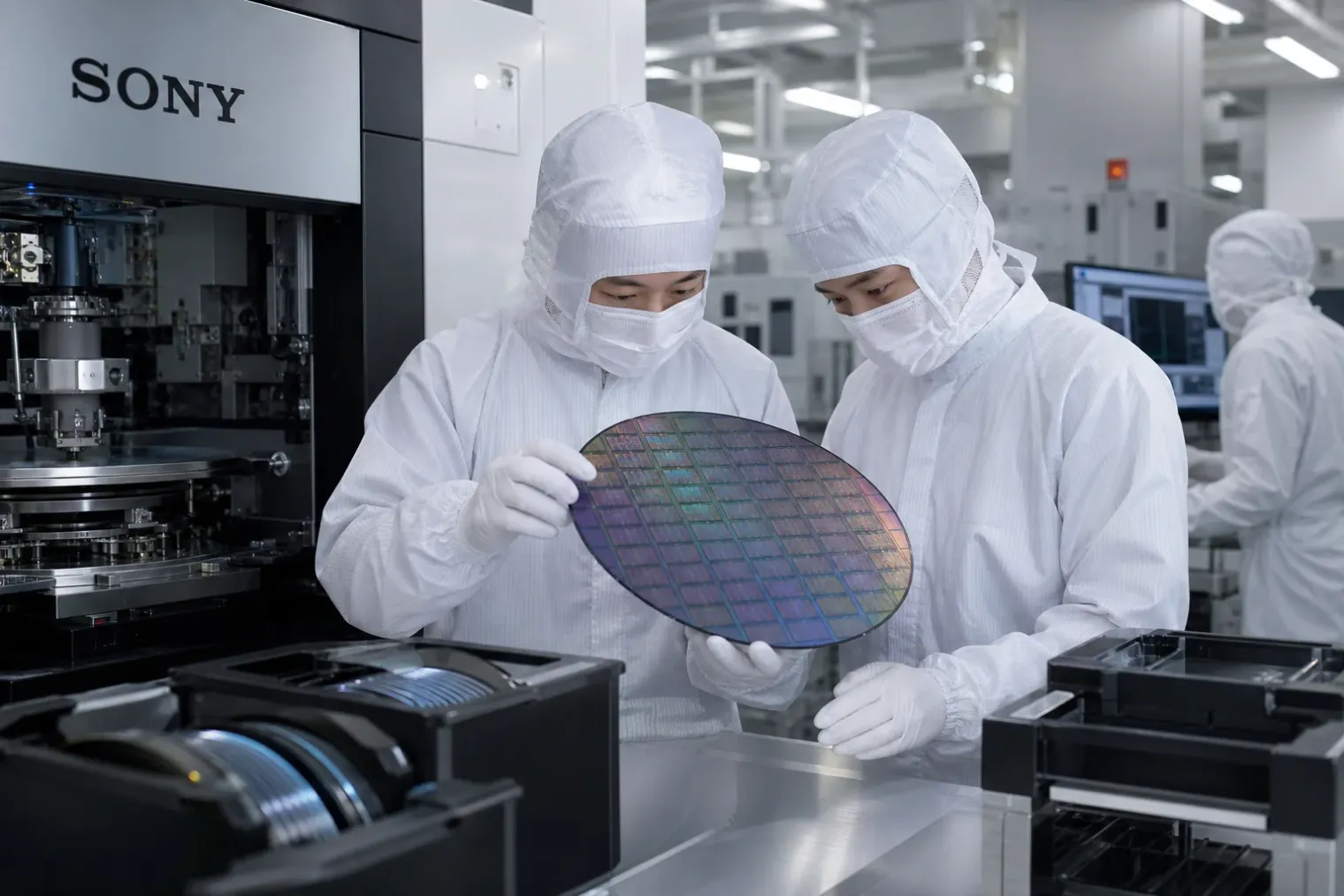
The proposed venture would set up development and production lines in Sony’s newly constructed facility in Koshi City, Kumamoto Prefecture. The location places the plan within the same regional semiconductor cluster that has become central to Japan’s effort to reinforce domestic chip production.
Sony and TSMC already have a history in Kumamoto through Japan Advanced Semiconductor Manufacturing, TSMC’s local manufacturing subsidiary. That earlier investment created a practical foundation of suppliers, engineering talent and government engagement in the area. The planned sensor venture is structurally different, however: Sony is expected to be the controlling shareholder, while TSMC would bring process technology and manufacturing expertise to a business based in Sony’s own new facility.
The companies said potential investment by the venture is under discussion. Sony is also considering further capital expenditure at its existing Nagasaki plant. Both the venture investment and Sony’s separate plant investment are being considered in phases according to market demand and on the assumption of Japanese government support. This approach limits the certainty of the project’s ultimate scale, but gives the partners flexibility to expand as orders and technical requirements become clearer.
Why sensor production needs closer integration
An image sensor is more than a light-sensitive pixel array. Modern CMOS sensors combine pixel technology, analogue circuitry, logic functions and packaging in increasingly complex stacked structures. Better performance depends on how those elements work together: light capture, dynamic range, noise control, power consumption, processing speed and the ability to operate reliably in difficult environments all affect the value of the finished component.
Sony’s established strengths lie in image-sensor architecture, pixel technologies and integration. TSMC brings process-development and production capabilities that can help translate demanding designs into manufacturable products at scale. Sony has described the division of capabilities in its existing model as Sony handling pixel technology, foundries such as TSMC producing logic, and Sony completing final sensor integration. A closer manufacturing partnership could reduce the hand-offs involved in that process and give both sides a more direct route to optimise future products.
This does not necessarily signal a departure from smartphone cameras or conventional digital imaging. Those markets remain important applications for image sensors. But the stated emphasis on “physical AI” points to a broader set of opportunities where cameras are inputs to machines rather than merely tools for recording images.
The industrial case: automotive and robotics
Sony and TSMC specifically identified automotive and robotics as areas for exploration. In these applications, sensors must supply consistent visual information to systems that identify objects, estimate distances, monitor environments or guide equipment. The requirements can differ from those of a mobile camera: low-light behaviour, high dynamic range, latency, power use, robustness and functional reliability can be as significant as maximum resolution.
The opportunity is therefore not simply to ship more camera chips. It is to support sensing hardware designed for machines that must interpret changing real-world conditions. That includes vehicle systems, industrial automation and robotics, although neither company has named initial customers or products.
Sony’s wider activity underlines this direction. In July 2026, Sony Semiconductor Solutions agreed with Mitsubishi Electric to create a separate venture for AI vision-sensor solutions in manufacturing, subject to regulatory approvals. That arrangement is distinct from the TSMC proposal, but it illustrates Sony’s effort to connect image-sensor technology to industrial decision-making and control systems.
A capital and execution test
The proposed partnership offers Sony a way to share the technical and financial demands of future sensor manufacturing while retaining control of the venture. For TSMC, it would extend a longstanding customer relationship into a more specialised manufacturing collaboration. The model could be particularly relevant as sensor designs require more sophisticated logic layers and tighter integration between device design and wafer production.
There are still material uncertainties. The companies have not disclosed the intended process technologies, the scope of the production lines, the targeted end markets, expected capacity or the financial contribution of either side. Government support is contemplated rather than confirmed. The venture also remains conditional on negotiations producing a definitive agreement.
For now, the announcement is best understood as a strategic commitment rather than an operating-company launch. Its importance lies in the direction it sets: Sony is seeking to protect and extend its imaging position as cameras become core sensors for automated systems, while TSMC is positioning its manufacturing expertise closer to a specialist, high-value semiconductor category. The next meaningful milestones will be a binding agreement, investment details and a timetable for bringing the Kumamoto operation into production.
Sources
- Sony Semiconductor Solutions and TSMC Enter Preliminary Agreement for Next-Generation Image Sensor Strategic Partnership — Sony Semiconductor Solutions
- Latest News — TSMC
- Sony Group Corporate Strategy 2026 — Sony Group Corporation
- Corporate Strategy and Earnings Announcement Presentation Q&A (Summary) — Sony Group Corporation
- Sony, TSMC Plan New Japan Joint Venture for Next-Generation Image Sensors — Reuters


