
A hiring signal, not a finished memory strategy
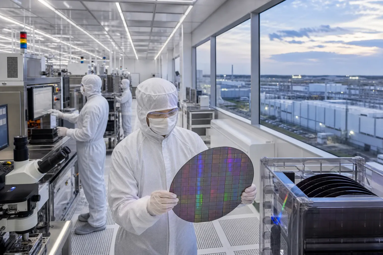
Tesla is recruiting semiconductor process engineers for Terafab, the proposed manufacturing programme backed with SpaceX. The roles are significant because they explicitly cover memory alongside logic, chip packaging, testing and lithography-mask work. One Austin-based wet-etch engineering vacancy says its processes would support edge-inference processors, radiation-resistant satellite chips and high-bandwidth memory.
That is more concrete evidence of a memory manufacturing ambition than general statements about a giant chip factory. Process engineers determine how a wafer is cleaned, etched, deposited, measured and controlled across thousands of production steps. Their work has a direct effect on defects, yield and reliability, which are decisive to whether a fab can turn laboratory processes into viable volume output.
Still, the vacancies should be read as an early operational indicator rather than proof that Tesla and SpaceX have solved the problem of building a major memory supplier. Recruiting for process development is a necessary first step for any fab, but it is far removed from qualifying equipment, establishing repeatable yields, building an ecosystem of materials suppliers and producing enough chips at competitive cost.
Terafab’s unusual integrated model
The plan presented for Terafab is unusually broad. Tesla’s recruitment material describes a vertically integrated facility intended to put logic, memory, packaging, testing and mask production under one roof. The companies have since outlined an initial Terafab phase in Grimes County, Texas, with investment of $16.8 billion and more than 100 million square feet of planned manufacturing space when the wider project is developed.
Combining these activities could offer practical advantages for products designed primarily for affiliated customers. Tesla, SpaceX and xAI require large quantities of specialised computing hardware for vehicles, robotics, AI training and inference, satellite systems and data-centre operations. Closer coordination between chip design, manufacturing and packaging could shorten feedback cycles when designs need revision.
The model also departs from the highly specialised structure of the global semiconductor industry. Leading logic foundries, memory makers, outsourced packaging companies and equipment suppliers typically operate as separate businesses with deep expertise in narrower stages of production. A campus that seeks to integrate all of them assumes that co-location and faster iteration can outweigh the benefits of that specialisation.
The distinction matters particularly for memory. Logic chips and DRAM require different manufacturing know-how, while high-bandwidth memory adds another challenge: multiple DRAM dies must be stacked and connected through advanced packaging. A role that combines memory-related process work with a wider fab programme therefore suggests a wish to control a strategically important part of the AI hardware stack, not merely to assemble purchased memory with internally designed processors.
Why high-bandwidth memory is the important clue
The strongest detail in the Tesla advertisement is its reference to high-bandwidth memory rather than memory in the abstract. High-bandwidth memory is used close to AI accelerators where data must move rapidly between compute and memory. It has become strategically valuable because large AI systems can be constrained not only by the availability of processors, but also by the volume, bandwidth and power efficiency of the associated memory.
That does not necessarily mean Terafab will soon manufacture commodity DRAM for PCs, smartphones or the broader merchant market. Tesla’s public hiring language points more directly to memory designed for its own high-performance computing systems. Such a focus would be consistent with the stated aim of supporting inference processors and space-oriented chips, where tightly integrated hardware may have more value than competing for general-purpose memory sales.
It is also possible that the project will rely on partnerships, purchased wafers or external packaging at stages of its development. The recruitment material establishes that Tesla wants engineers capable of developing memory processes. It does not disclose a product roadmap, a process node, planned wafer capacity, a qualified equipment base or a schedule for commercial memory shipments.
Scale, financing and execution risks
Terafab’s proposed scale makes its execution more consequential and more uncertain. Local public documents connected to the Grimes County project previously described much larger potential capital investment over successive phases than the announced initial commitment. This illustrates the gap between a first construction phase and a fully realised semiconductor campus.
The financial requirements are likely to extend well beyond buildings and land. Advanced fabs need expensive lithography, deposition, etch, inspection and metrology tools, as well as reliable supplies of ultra-pure chemicals, gases, wafers and spare parts. They also require substantial electricity, water treatment, cleanroom infrastructure and a workforce with experience in process integration and yield improvement.
Memory manufacturing adds another layer of exposure: it is historically cyclical. Prices and margins can rise sharply during shortages, then fall when supply expands or demand weakens. Micron’s fiscal 2023 results offer a recent illustration of that volatility. The US memory producer reported a GAAP net loss of $5.83 billion after industry demand and pricing deteriorated, despite its established technology, customer base and manufacturing network.
A new entrant can justify investment by securing internal demand, but captive demand does not automatically guarantee low costs or high yields. If Terafab is principally an internal supplier, its success will depend on whether the chips it produces improve the availability, performance or economics of Tesla and SpaceX systems compared with buying from existing leaders.
What the recruitment actually changes
The immediate conclusion is narrower than claims that Musk is about to become a major memory manufacturer. Tesla’s job listings confirm that Terafab is assembling expertise across core semiconductor process disciplines and that high-bandwidth memory is part of the technical scope. The more recent Texas project announcement shows that the effort has progressed from a conceptual proposal to a defined initial investment and site plan.
But the decisive milestones lie ahead. Observers should look for confirmed equipment orders, construction progress, further hiring in memory integration and packaging, supplier agreements, process qualification and, eventually, evidence of reliable output. Until then, Terafab is best understood as a serious attempt to build semiconductor capability around Musk’s companies’ AI ambitions, rather than as an established challenger to the world’s memory manufacturers.
Sources
- Musk explores memory production and seeks memory-process engineers — Diit.cz
- Sr. Process Engineer, Wet Etch, Terafab — Tesla
- Elon Musk's massive Terafab chip-making facility starts to take shape — Tom's Hardware
- Notice of Public Hearing: SpaceX Reinvestment Zone No. 1 — Grimes County, Texas
- Micron Technology reports fourth-quarter and full-year fiscal 2023 results — Micron Technology


