
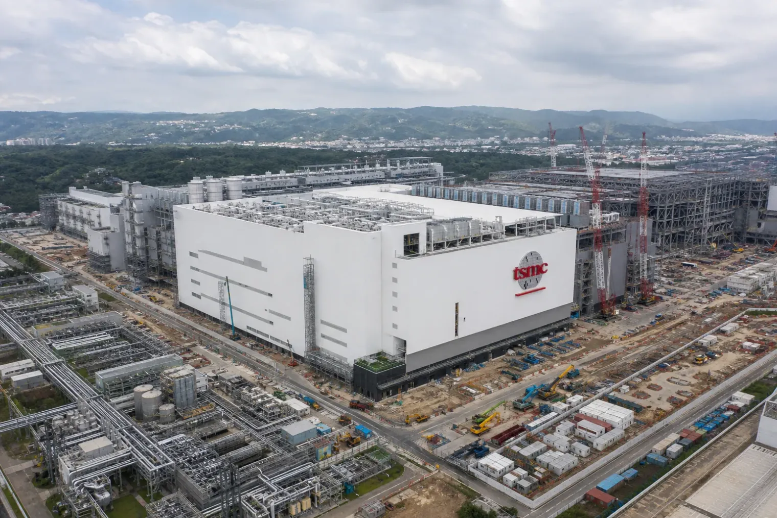
A construction milestone, not chip volume production
TSMC’s first fab intended for its A14, or 1.4-nanometre-class, manufacturing technology is reportedly expected to be structurally completed by April 2027 at the Central Taiwan Science Park in Taichung. The date is significant because it suggests the building programme is progressing quickly enough to support equipment installation and process qualification ahead of TSMC’s stated 2028 production target.
The distinction matters. Completion of a semiconductor fab does not mean it is ready to manufacture commercial chips. After civil construction, a facility must be fitted with highly specialised cleanroom systems, utilities, production tools and process-control equipment. Those systems then require extensive installation, testing and qualification before pilot wafers can be run. Only later can a plant move into high-volume manufacturing.
TSMC has not publicly presented April 2027 as a formal corporate production milestone. Its official disclosures instead confirm that it began construction of a 1.4-nanometre fab in Taichung during 2025 and that A14 volume production is scheduled for 2028. The reported completion date should therefore be read as an indicator of construction progress rather than a change to the company’s official technology roadmap.
Why the Taichung project matters
The proposed A14 production site reinforces Taiwan’s central role in TSMC’s leading-edge operations. The company has expanded manufacturing abroad in the United States, Japan and Europe, but it continues to concentrate its newest process development and the first stages of advanced-volume capacity in Taiwan.
That concentration is operational as well as strategic. Moving a new node from development to commercial production depends on close coordination between research teams, equipment suppliers, materials specialists, packaging operations and the manufacturing organisation. Locating early capacity near the wider Taiwanese semiconductor ecosystem can reduce the delay between identifying a yield issue and applying a production fix.
The A14 fab also sits within a broader wave of Taiwanese investment. TSMC is expanding 2-nanometre capacity in Hsinchu and Kaohsiung, adding 3-nanometre capability in Tainan, and building further advanced-packaging capacity. Together, these projects show that the industry’s bottleneck is no longer limited to transistor fabrication. Advanced packages, high-bandwidth memory integration, power delivery and data movement are increasingly important for AI and high-performance computing systems.
A14 is about more than a smaller label
The “1.4-nanometre” description is a process-family name rather than a literal measurement of every chip feature. It nevertheless signals a new generation of manufacturing technology beyond TSMC’s 2-nanometre platform.
TSMC has said that A14 is designed to offer higher speed, lower power consumption and greater logic density than N2, its first 2-nanometre-generation process. The company has also described A14 as using second-generation nanosheet transistor technology and an enhanced standard-cell architecture. These changes are intended to give chip designers more flexibility in balancing performance, power use and area.
That balance is especially relevant for AI accelerators and data-centre processors. Their performance is constrained not only by transistor speed, but by power budgets, cooling capacity, memory bandwidth and the ability to combine multiple large dies in a single package. A denser and more efficient logic process can help, but it is only one component of the finished system.
TSMC’s roadmap places A14 in production during 2028, while an A14-based 3D stacking option is planned for 2029. That sequencing illustrates a wider industry direction: advances in front-end transistor scaling are being paired with increasingly sophisticated back-end integration rather than replacing it.
The schedule remains demanding
An April 2027 building-completion goal would leave a relatively compressed period before A14 production is due to begin in 2028. Such timing is possible in a well-established manufacturing cluster, but it leaves little room for disruption in tool delivery, utility commissioning, cleanroom validation or process transfer.
The challenge is heightened by the scale and complexity of leading-edge fabrication. Modern fabs require large quantities of reliable electricity and ultra-pure water, tightly controlled chemical handling and a supply chain capable of maintaining precision tools. Leading-edge lines also depend on advanced lithography equipment and a dense network of specialist suppliers.
TSMC’s experience with earlier node transitions reduces some execution risk. Its 2-nanometre technology entered volume production in late 2025, providing a production base for nanosheet transistors before A14 is introduced. Still, each new node requires its own yield learning, design rules and customer validation. Progress in the building programme alone cannot establish whether commercial A14 yields will meet the company’s objectives.
What to watch next
The most useful confirmation points will be tool-installation progress, pilot-wafer activity and customer design announcements. A move from completed construction to equipped cleanrooms would make the reported April 2027 date more meaningful. Pilot production in the second half of 2027, if achieved, would then support TSMC’s public objective of beginning A14 volume production in 2028.
For customers, the practical question is not simply when the fab is finished, but when qualified A14 capacity becomes available in sufficient volume for new processors. For the wider industry, the Taichung build is a measure of whether TSMC can maintain its cadence of process advances while simultaneously expanding capacity across several regions and investing heavily in advanced packaging.
The reported construction milestone is therefore best seen as an early operational signal. It supports the credibility of TSMC’s 2028 A14 plan, but it does not remove the technical and manufacturing work still required before 1.4-nanometre-class chips reach the market.
Sources
- TSMC's 1.4 nm Fab Set for Completion by April 2027 — TechPowerUp
- GIGAFAB Facilities — TSMC
- TSMC Debuts A13 Technology at 2026 North America Technology Symposium — TSMC
- 2025 Annual Report — TSMC
- TSMC accelerates work on future chips as the fab progresses — Tom's Hardware Italy


