
A competitive claim that needs qualification
Reports that TSMC is developing an EMIB-like packaging technology point to a real shift in the economics and engineering of artificial-intelligence processors. Intel’s Embedded Multi-die Interconnect Bridge, or EMIB, has become a more visible alternative to the large silicon interposers used in much of TSMC’s CoWoS packaging portfolio. Yet the available public record does not show TSMC announcing a one-for-one EMIB equivalent.
Instead, TSMC has described a multi-track strategy: increasing the size of its established CoWoS packages, extending wafer-level system integration, and developing Chip-on-Panel-on-Substrate, or CoPoS. That distinction matters. An “EMIB-like” label is a useful shorthand for the competitive pressure around large chiplet packages, but it can obscure meaningful differences in architecture, maturity and intended use.
The contest is increasingly about how to combine many compute dies, high-bandwidth memory stacks and input/output components into one reliable package. As chipmakers confront the physical limits of producing ever-larger monolithic processors, packaging has become a central performance technology rather than a back-end manufacturing step.
Why EMIB has become a significant alternative
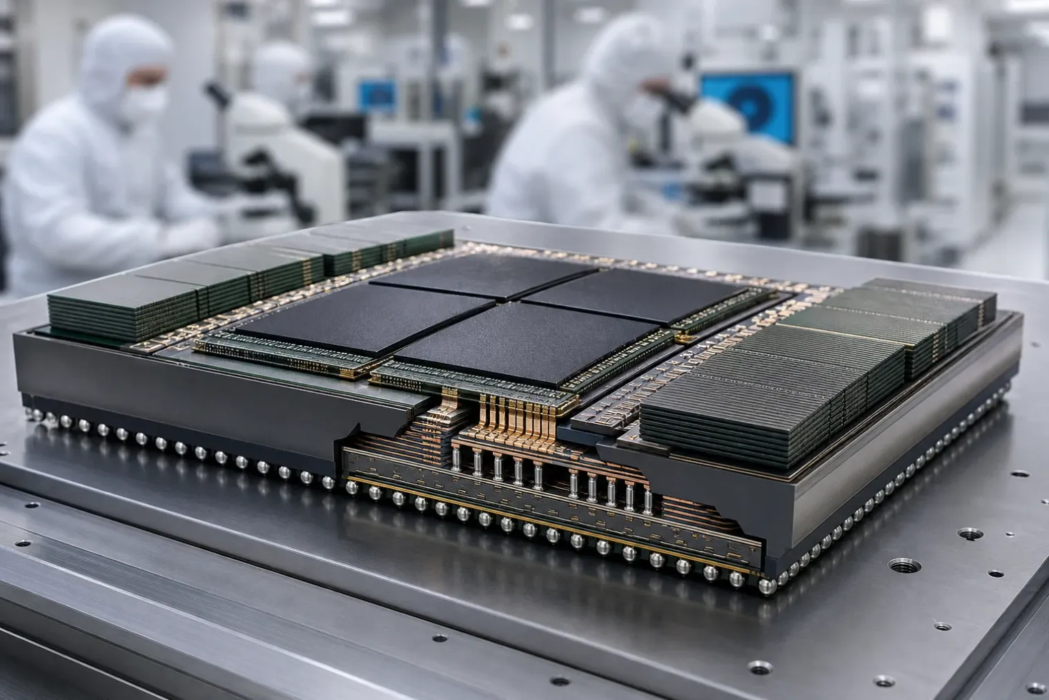
Intel’s EMIB uses small silicon bridges embedded in an organic package substrate. Rather than placing all connected dies on a single, full-size silicon interposer, the approach concentrates fine interconnects where neighbouring dies need them. Intel argues that this can support heterogeneous integration while avoiding some of the area, routing and cost implications of a large interposer.
This architecture is particularly relevant to the biggest AI accelerators. These devices must connect large compute chiplets to multiple stacks of high-bandwidth memory while sustaining enormous data flows and managing power delivery. An embedded bridge can be an attractive option where designers need local, dense die-to-die links without extending fine-pitch silicon across the entire package.
Intel has also developed newer EMIB variants for more demanding power and memory configurations. Its current technology material describes bridges with through-silicon vias for vertical power delivery, as well as combinations of EMIB with Foveros die stacking. The company’s central proposition is flexibility: customers can use different bridge configurations for different connections within a complex package.
That does not make EMIB universally superior to interposer-based packaging. System designers must weigh interconnect density, power integrity, thermal behaviour, manufacturing yield, layout freedom, ecosystem support and total cost. The appropriate package depends on the particular accelerator, memory configuration and production volume.
TSMC’s response is scale, capacity and optionality
TSMC’s starting position remains strong. CoWoS is widely used for high-performance computing and AI packages, and the company is already producing 5.5-reticle-size CoWoS designs in 2026. Its stated roadmap extends to a 14-reticle package in 2028, designed to integrate about 10 large compute dies and 20 high-bandwidth-memory stacks, followed by still larger configurations in 2029.
The immediate competitive advantage of this approach is continuity. Customers that have built products, design flows and supply relationships around CoWoS can scale within a familiar platform. TSMC is also combining packaging with its wider manufacturing and design ecosystem, including front-end process technologies, 3D stacking and interconnect options.
At its April 2026 earnings call, TSMC directly acknowledged the competition from substrate-based alternatives such as EMIB. Management said the company was developing very large-reticle packaging technologies and confirmed that CoPoS was under development. However, it also said that large-format CoWoS remained the main supply approach in the near term.
This is the clearest public indication of TSMC’s strategic position: it is not relying on one response to Intel. It is protecting the current CoWoS franchise through larger interposers and additional capacity, while investing in panel-based packaging for the next phase of scaling.
CoPoS addresses a related problem, not necessarily the same one
CoPoS replaces the wafer-sized manufacturing format used in conventional advanced packaging with a much larger panel format. The potential appeal is scale. Larger panels can create more physical area for package assembly and may improve the economics of very large packages once manufacturing processes mature.
But CoPoS should not automatically be treated as an EMIB substitute. EMIB is defined by locally embedded silicon bridges in the substrate. CoPoS is principally a panel-based packaging architecture. Both address the need to build larger chiplet systems, but they approach that objective differently.
TSMC has indicated that CoPoS remains a longer-term project. The company is building a pilot line, with production expected a couple of years later, while industry observers expect a broader manufacturing ramp in the 2028–2029 period. TSMC executives have also cautioned that panel-based technologies will not initially match wafer-level packaging for interconnection density. Consequently, CoPoS is more likely to complement CoWoS than abruptly replace it.
Capacity remains as important as technical design
The competitive backdrop is not purely architectural. Advanced packaging capacity has been constrained by demand for AI infrastructure, and TSMC has repeatedly said that its high-end packaging supply is tight. Expanding it involves long lead times for facilities, tools, materials and qualified manufacturing processes.
This creates an opening for Intel and other packaging suppliers. A chip designer may consider an alternative not because it considers CoWoS technically inadequate, but because it wants a second qualified source, a different package geometry, regional manufacturing diversity or available capacity. Conversely, moving an established accelerator from one packaging architecture to another is not a simple sourcing decision. It can require significant redesign, qualification and supply-chain work.
For TSMC, the important issue is therefore not whether it copies EMIB precisely. It is whether its portfolio provides customers with competitive options in package size, bandwidth, power delivery, cost and production availability. Its public plans suggest that it is pursuing all of those dimensions simultaneously.
The emerging packaging rivalry
The headline claim that TSMC is developing an EMIB-like technology captures a broader truth: Intel’s embedded-bridge approach has become important enough that TSMC is addressing the same market requirements openly. Still, the public evidence supports a more nuanced conclusion. TSMC is advancing CoWoS, wafer-level integration and CoPoS rather than presenting a formally branded EMIB analogue.
The next several years will determine whether the market settles around a dominant packaging model or becomes more fragmented. For AI chip customers, a wider choice of advanced packaging technologies could reduce bottlenecks and improve bargaining power. For TSMC and Intel, the prize is not simply technical prestige. It is a larger share of the value created when an AI processor becomes a complete computing system.
Sources
- TSMC Develops EMIB-like Technology to Compete with Intel — TechPowerUp
- TSMC First Quarter 2026 Earnings Call Transcript — TSMC Investor Relations
- TSMC Debuts A13 Technology at 2026 North America Technology Symposium — TSMC
- EMIB Technology Brief — Intel
- TSMC Accelerates CoPoS Development — TrendForce


