
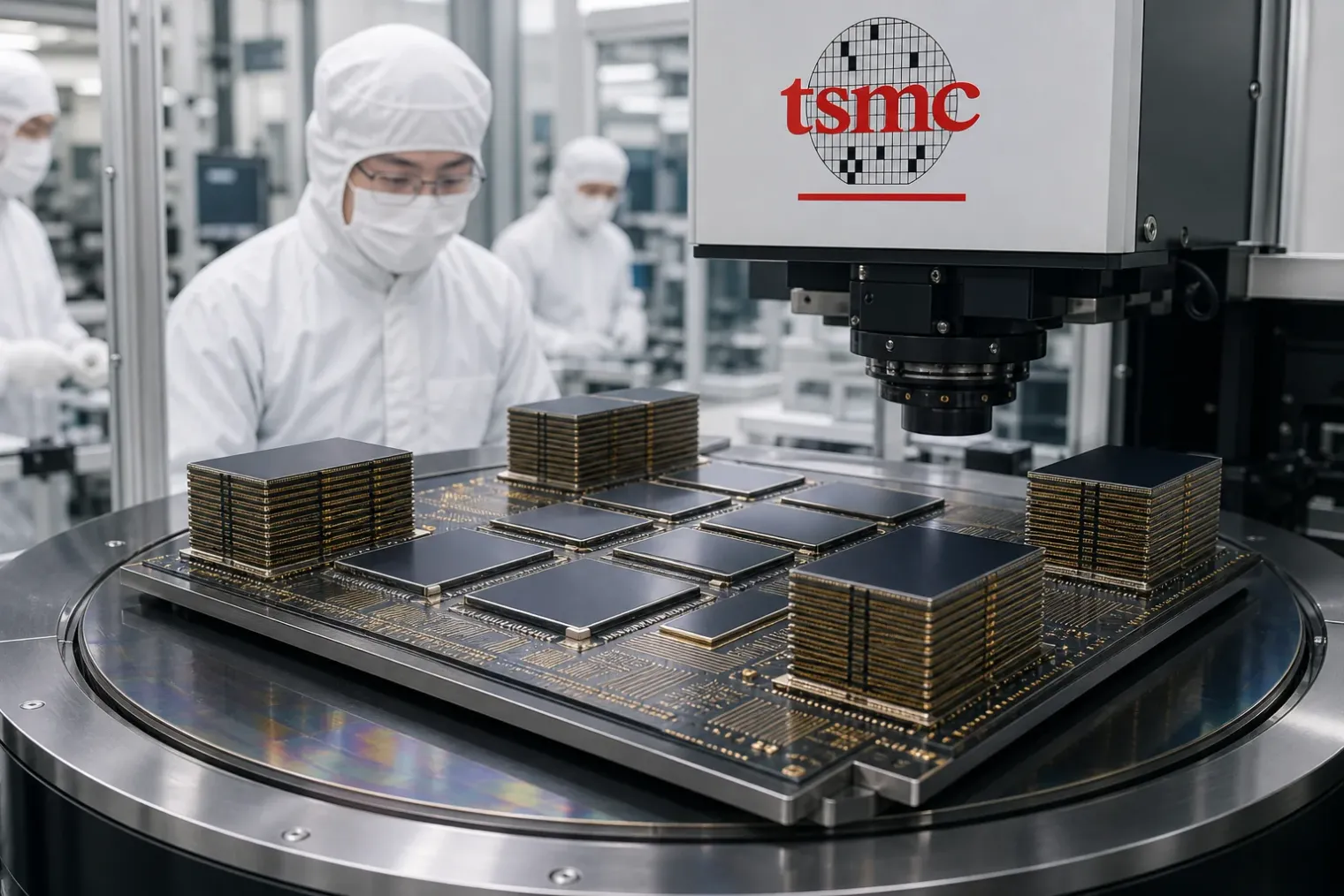
A packaging milestone rather than a conventional chip yield claim
TSMC says it has put its 5.5-reticle-size CoWoS advanced packaging technology into volume production in 2026, with yield exceeding 98%. The result matters because advanced packaging has become a central constraint on the supply and capability of large artificial-intelligence accelerators: it is the layer that combines logic dies, chiplets and high-bandwidth memory into a single system.
The headline requires one important clarification. TSMC’s disclosed roadmap indicates that a 14-reticle CoWoS platform, supporting up to 20 high-bandwidth-memory stacks, is targeted for production in 2028. A package larger than 14 reticles, designed for up to 24 HBM stacks, is planned for 2029. Therefore, the 2029 date applies to the next expansion beyond 14 reticles, rather than to the first 14-reticle implementation.
The reported yield is significant because the 5.5-reticle format is far larger than the area that can be exposed in one lithography field. Producing such a package requires the integration of multiple large components while maintaining reliable electrical connections, mechanical integrity and acceptable thermal behaviour. A high manufacturing yield at this scale can make architectures that were previously technically possible but commercially difficult more practical.
Why CoWoS-L is central to AI hardware
CoWoS, short for Chip-on-Wafer-on-Substrate, is TSMC’s family of 2.5D packaging technologies. It places multiple components close together on an interposer, enabling dense, high-speed links between compute silicon and HBM. This approach allows designers to move beyond the practical limits of a single monolithic processor die.
The CoWoS-L variant combines redistribution layers with local silicon interconnects. In broad terms, that gives designers a way to use silicon only where very dense die-to-die routing is needed, while using a larger moulded interposer structure to extend the package. The model is intended to scale package area without requiring one enormous silicon interposer.
TSMC’s own technology material shows the progression clearly. Its 3.5-reticle CoWoS-L entered volume production in 2024. The company completed certification of 5.5-reticle interposers in 2025 and said it would start volume production in 2026. The latest reported yield suggests that this transition has moved beyond qualification into a manufacturing state suitable for customer products.
That distinction is consequential for AI chip suppliers. Generative-AI training and inference systems increasingly depend on very large pools of HBM located close to compute dies. More package area can support more memory stacks, more processing chiplets or both. It also allows system architects to pursue higher aggregate memory bandwidth without moving as much traffic across slower board-level connections.
Reading the 98% figure carefully
A yield above 98% is an impressive manufacturing assertion, but it should not be interpreted as a complete measure of the yield of a finished AI accelerator. TSMC has not publicly specified the exact calculation, the product mix, the test stages included or the denominator used for this particular figure.
In semiconductor production, yield can refer to different stages: an interposer, a packaging assembly, a wafer, an individual die or a fully tested module. The eventual usable output of an accelerator depends on the compounded performance of every constituent element, including leading-edge logic dies, HBM devices, interconnects, substrates and final testing. A package-level yield does not eliminate the possibility of losses elsewhere in that chain.
Nor is it a straightforward benchmark against quoted yields for a rival’s manufacturing process. Different technologies have different defect sensitivities, component counts, test criteria and maturity levels. The more defensible conclusion is that TSMC is reporting a high level of process control for a very large advanced-package format, rather than that it has established an industry-wide yield comparison.
Still, the result is commercially meaningful. Large multi-die modules are exposed to a compounding problem: each added die, memory stack and connection creates another potential source of failure. Improving assembly yield limits scrap costs and helps suppliers plan volume shipments more confidently. This is particularly important in a market where packaging capacity, HBM availability and power delivery are all potential bottlenecks.
Scaling shifts from transistors to systems
The development illustrates how semiconductor scaling is becoming increasingly system-oriented. Smaller process nodes remain important, but growing a processor through packaging has become equally vital for workloads that demand extreme memory bandwidth and massive parallel computing capacity.
TSMC has framed its roadmap as a combination of CoWoS, System-on-Wafer technology and related 3D integration methods. CoWoS remains the near-term route for very large accelerator packages, while wafer-scale integration could support even larger systems later. The company is also developing co-packaged optics, which aims to bring optical links closer to switching and computing silicon as conventional electrical interconnects face bandwidth and power limitations.
The 5.5-reticle milestone should therefore be seen as an intermediate point rather than an endpoint. TSMC’s public plans call for annual advances in packaging scale, culminating in the 2028 14-reticle platform and a larger-than-14-reticle format in 2029. Those future products will face harder challenges in substrate flatness, warpage control, thermal dissipation, power delivery, test coverage and supply-chain coordination.
The remaining constraints
A successful packaging yield does not by itself guarantee abundant AI hardware. HBM supply remains a major determinant of how many top-end accelerators can be assembled, while large packages require sophisticated substrates and increasingly demanding cooling solutions. As packages grow, power density and heat removal become more difficult engineering problems for both chip suppliers and data-centre operators.
There is also an economic constraint. Larger packages can improve performance and reduce communication overhead, but they tie together a greater value of components in every assembly. Manufacturers must maintain high yields across logic, memory and packaging to prevent a fault in one part from turning an expensive module into scrap.
TSMC’s reported 98%-plus CoWoS yield indicates that its packaging process has cleared an important industrial threshold for the current generation of large AI systems. The more consequential test now is whether the company can repeat that manufacturing discipline as package size, HBM counts and power requirements increase through 2028 and 2029. For the AI hardware market, the capacity to assemble the largest systems reliably may prove as strategically important as the ability to fabricate the most advanced transistors.
Sources
- TSMC Achieves 98% Yield on CoWoS-L with 5.5x Reticle Size, 14x Comes in 2029 — TechPowerUp
- TSMC 2025 Annual Report — TSMC
- CoWoS — TSMC
- TSMC touts advanced packaging, 2nm progress at tech symposium — Focus Taiwan
- TSMC Tech Symposium 2026, By The Numbers — Semiconductor Engineering


