
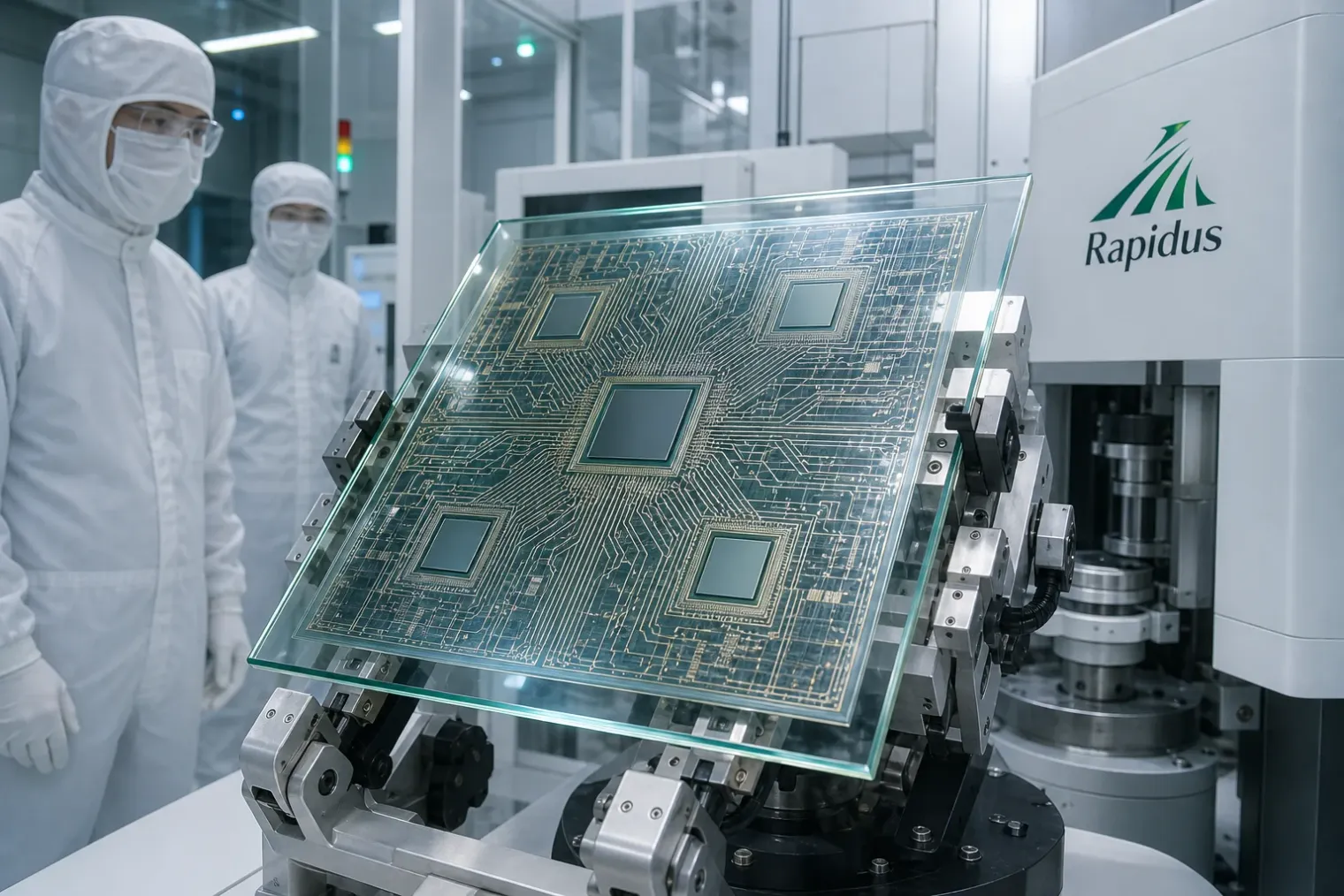
Packaging is becoming the scaling problem
Rapidus is positioning advanced packaging, rather than transistor fabrication alone, as a central constraint on the next generation of artificial-intelligence and high-performance-computing processors. Its stated target is an eight-reticle interposer, assumed to be roughly 81 mm by 81 mm, produced using 600 mm by 600 mm panel-level packaging technology by 2030.
The proposition responds to a basic change in semiconductor design. Instead of building every function into one increasingly expensive monolithic die, system designers can combine compute chiplets, input-output dies and stacks of high-bandwidth memory in one package. This approach can improve design reuse and yield while allowing different parts of a processor to use different manufacturing processes. It also shifts a larger share of engineering difficulty into the package: the components must exchange enormous volumes of data over short, dense and reliable connections.
For the largest processors, the interposer is the enabling layer. In a 2.5D package, it supplies dense wiring between side-by-side dies and memory stacks. As the number of chiplets and memory devices rises, that interposer must become larger. Conventional 300 mm silicon wafers are poorly suited to making very large square interposers efficiently, because the number of usable units per wafer falls quickly and edge losses become more significant.
Why a 600 mm panel changes the arithmetic
Rapidus argues that a 300 mm wafer can yield only four eight-reticle interposers, whereas a 600 mm square panel could yield about 49. This comparison illustrates the strategic logic of panel-level manufacturing: a square panel is a more efficient starting shape for a large square substrate than a circular wafer.
The advantage is not merely the gross area of the panel. A 600 mm square format has four times the surface area of a 300 mm square, while a 300 mm circular wafer has materially less area than a 300 mm square. More importantly, large square interposers fit into a square panel in a regular grid. The resulting reduction in unused perimeter area could matter greatly when each package substrate is large and expensive.
Rapidus’s approach uses glass panels and redistribution-layer interposers rather than assuming that every large interposer must be made from silicon. Redistribution layers are metal wiring layers formed on a carrier or substrate that can route signals among chiplets and memory. Glass offers attractive properties for this role: dimensional stability, a flat surface, electrical insulation and potentially lower signal loss at high frequencies. It can also be produced in large formats.
The company’s broader roadmap links this work to an integrated model in which it develops leading-edge logic manufacturing and advanced packaging together. Rapidus has said that it intended to open a chiplet packaging pilot line near its IIM-1 fabrication site in Chitose, Hokkaido, in April 2026. The relevant distinction is important: a pilot line demonstrates process capability, while stable high-volume output with acceptable yields and reliability is the much harder commercial milestone.
An ambitious point on an industry-wide curve
The eight-reticle objective is aggressive, but it reflects a wider packaging race rather than an isolated bet. TSMC’s established CoWoS platform has expanded beyond traditional silicon-interposer dimensions. Its current public materials describe production-qualified 5.5-reticle interposers, with volume production planned for 2026, while its technology portfolio also uses redistribution-layer interposers for configurations larger than a 3.3-reticle silicon interposer.
That comparison puts Rapidus’s target in context. An eight-reticle package would not be a small incremental increase over available technology. It would require a manufacturing platform designed around much larger substrates, exceptionally precise patterning and placement, and stable electrical performance across a very large area. Yet the direction of travel is clear: AI accelerators require more compute, more memory and more bandwidth, all within power and physical constraints that conventional board-level assembly cannot satisfy.
The plan also suggests that panel-level packaging may become a competitive differentiator for foundries. Historically, advanced packaging has involved a mixture of foundries, outsourced semiconductor assembly and test providers, substrate makers, materials suppliers and equipment vendors. A company able to tightly couple logic process technology, design rules and a packaging platform could offer customers a more integrated route from chip architecture to finished system package.
That potential advantage will depend on whether Rapidus can supply more than a large physical format. Customers will require a complete ecosystem: design enablement, known-good-die strategies, test flows, thermal solutions, substrate supply, assembly capacity and long-term qualification data. Large AI packages also need practical power delivery and cooling. An interposer can solve routing density, but it cannot by itself remove the heat generated by multiple high-performance dies.
Glass improves some constraints while creating others
Glass is a promising material, not a universal answer. Its flatness and dimensional stability can help fine-pitch interconnect processes, and its electrical characteristics are appealing for high-speed signals. Unlike silicon, glass is electrically insulating, which can simplify some design choices. Panel processing also creates a credible path to larger formats and better material utilisation.
However, glass-based packaging imposes difficult manufacturing and reliability requirements. Large, thin panels must be handled without cracking or excessive warpage. Through-glass vias, metal adhesion and redistribution-layer formation must remain reliable through repeated thermal cycling. The coefficient of thermal expansion of the glass, the silicon dies, metals, moulding materials and package substrate must be engineered as a system. Small mismatches can produce stress, delamination or cracking over the life of the product.
Yield is the decisive variable. A larger panel may offer dramatically better theoretical output, but one defect can affect a large number of packages. The commercial benefit therefore depends on defect density, inspection capability, rework options, panel handling and the ability to keep patterning and assembly accurate from the centre to the edges. These are mature challenges in display and printed-circuit manufacturing, but leading-edge semiconductor packaging requires much tighter tolerances.
The significance of the 2030 target
Rapidus is not promising an immediate replacement for wafer-level interposers. Its 2030 goal should instead be read as a long-range manufacturing target aligned with expected growth in package dimensions. The company expects semiconductor packages to become two to three times larger by 2030, driven by AI, automotive and other compute-intensive applications.
If the programme succeeds, it could give Rapidus a differentiated manufacturing route for very large chiplet systems at a time when packaging capacity and substrate size are becoming strategic constraints. It could also help Japan build a more complete domestic semiconductor capability spanning fabrication, materials and advanced assembly.
The risk is equally clear. Rapidus must simultaneously establish leading-edge logic production, prove a new large-panel packaging flow and persuade customers to design products around an unproven manufacturing ecosystem. Eight-reticle interposers on 600 mm panels are therefore best understood not as a near-term product announcement, but as a declaration of where Rapidus believes the economics of AI packaging must go. The next evidence to watch will be pilot-line results, reliability qualification, customer design wins and the transition from demonstration panels to repeatable commercial yields.
Sources
- Rapidus Targets 8-Reticle Interposers on 600 mm Advanced Packaging Panels by 2030 — TechPowerUp
- Rapidus Merges Front-End and Back-End Semiconductor Processes for Ultimate Performance — Rapidus Corporation
- Business and Technologies — Rapidus Corporation
- HPC Platform – TSMC 3DFabric — TSMC
- Glass Core Substrate — IEEE Electronics Packaging Society


