
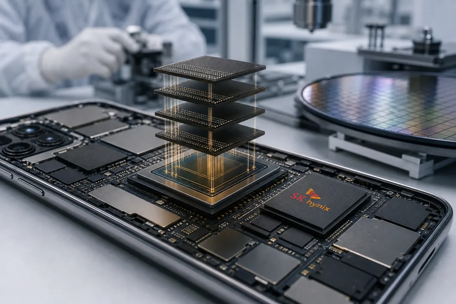
The important distinction behind the headline
The prospect of faster local AI in smartphones is real, but the technology described in recent reporting requires a careful distinction. SK hynix has signalled work on 3D-stacked DRAM placed directly on logic, an architecture intended to reduce the distance between processing and memory. WMCM, or wafer-level multi-chip module, is a different advanced-packaging term associated in industry reporting with TSMC and with rumours surrounding future Apple processors.
That distinction matters because packaging has become as consequential to chip performance as transistor scaling. On-device AI workloads repeatedly fetch model parameters from memory while running calculations on a CPU, GPU or neural processor. If data cannot move quickly and efficiently enough, adding compute performance brings diminishing returns. A better physical relationship between memory and logic could therefore address a central mobile-AI constraint: feeding the processor without exhausting the phone’s power and thermal budgets.
SK hynix has not announced a retail smartphone product based on this approach, nor has it identified a customer. What it has done is describe a direction of travel that could alter how future mobile processors are assembled.
From package-on-package to memory on logic
Most smartphone processors use package-on-package construction. The application processor and memory are packaged as separate components and stacked together. The approach is well established, compact and highly manufacturable, but it retains an electrical interface between the logic package and memory package.
SK hynix’s proposed 3D DRAM-on-logic concept goes further. DRAM would be vertically integrated directly above a system-on-chip or other logic die. In principle, that can shorten connections, support many more input/output paths within the same footprint and reduce the energy used to move each bit of data.
The expected benefits are higher memory bandwidth, lower latency and better space efficiency. These are particularly relevant for local generative AI, image processing and other workloads that handle large models or frequent transfers of intermediate data. A phone could potentially perform more work locally, respond faster and depend less often on a remote server.
However, the potential advantage should not be reduced to a simple claim that more bandwidth automatically makes a phone’s AI more capable. Memory capacity, model optimisation, neural-processing hardware, software frameworks, battery capacity and cooling all remain decisive. Packaging can ease one bottleneck; it does not remove the wider system trade-offs.
Evidence of an early development effort
The strongest indication of SK hynix’s near-term intent is a San Jose job listing for a 3D Stacked DRAM Design Engineer. The posting says the company is seeking expertise to co-design logic dies with US-based customers for DRAM-on-logic configurations. That wording suggests a customer-specific development programme rather than a finished, standardised product ready for broad supply.
SK hynix had already placed the concept on its longer-term technology roadmap. At TSMC’s 2026 Technology Symposium, the company described closer integration of memory and logic as a route beyond the “memory wall” that constrains AI systems. It specifically identified 3D Stacked DRAM on Logic as a technology for improving bandwidth, latency, power efficiency and space use, with on-device AI among the intended applications.
This puts the development in an exploratory but strategically meaningful phase. Co-design is important because vertically integrated memory cannot be treated as a generic drop-in replacement for conventional mobile DRAM. The logic die, physical layout, thermal strategy, interfaces and software expectations all need to be considered together. That makes adoption more complex, but it may also allow a processor designer and memory supplier to achieve gains unavailable through standard components.
Why mobile AI is driving packaging innovation
AI has already made memory bandwidth a defining issue in data-centre accelerators, where stacked high-bandwidth memory is used beside powerful GPUs. Smartphones have fundamentally different limits: they must fit in a thin enclosure, run from a small battery and keep surface temperatures comfortable. Yet local AI creates a similar need to deliver large amounts of data to compute hardware efficiently.
SK hynix has been building a broader portfolio around this opportunity. At Mobile World Congress 2026, it displayed mobile-oriented LPDDR6, UFS storage and combined memory-storage packages alongside its data-centre products. The company’s public framing is that on-device AI needs a mixture of faster low-power memory and storage, rather than one universal component.
A 3D DRAM-on-logic product would represent a more radical step than those conventional mobile-memory upgrades. It could make high-bandwidth memory closer to the processor practical in a compact device, but engineering difficulties are substantial. Heat from the logic die must be managed without degrading the DRAM above it. Manufacturing yield and repairability can become more challenging as integration rises. The resulting product must also offer enough real-world efficiency to justify its likely higher cost.
WMCM remains a separate story
WMCM should not be attributed to SK hynix on the basis of the current evidence. Reports have linked the technique to TSMC’s packaging plans and to possible future Apple chips, describing an approach that integrates components such as a system-on-chip and DRAM at wafer level before the package is separated into individual units. Those reports remain dependent on supply-chain and analyst information rather than an Apple product announcement.
The two approaches share a broad objective: bringing memory and logic closer together to improve signal quality, bandwidth, energy use and package density. But they are not interchangeable names for the same technology, and the companies’ roles differ. TSMC is associated with wafer-level packaging and leading-edge logic manufacturing; SK hynix is advancing the memory-side architecture and customer co-design needed for stacked DRAM-on-logic systems.
For consumers, the outcome is not imminent proof of dramatically more intelligent phones. It is a sign that the industry sees memory movement, not only processor speed, as a limiting factor for the next stage of local AI. If SK hynix can translate its research into reliable, affordable products, the eventual effect may be smartphones that run larger or more responsive AI features locally while using less energy per task.
Sources
- Nové pouzdření čipů WMCM od SK hynix zvýší výkon lokálních AI v telefonech — Svět hardware
- 3D Stacked DRAM Design Engineer — SK hynix America
- SK hynix presents its vision at TSMC Technology Symposium 2026 — SK hynix Newsroom
- SK hynix Unveils Latest AI Memory Solutions at MWC 2026 — SK hynix Newsroom
- SK hynix Reportedly Hires for 3D-Stacked DRAM-on-Logic With a U.S. Customer — TrendForce


