
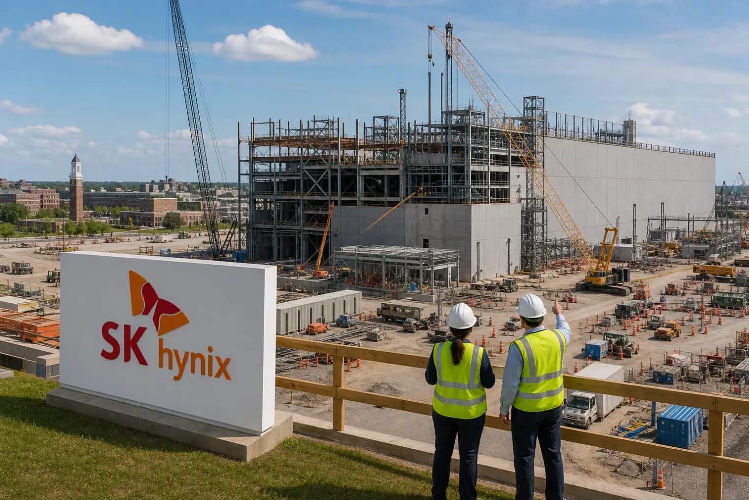
A milestone for US AI-memory capacity
SK hynix has held a groundbreaking ceremony for its advanced high-bandwidth memory packaging facility in West Lafayette, Indiana, putting physical construction behind one of the most consequential memory investments announced under the US semiconductor policy push. The South Korean company now expects the site to start mass-producing next-generation HBM in the second half of 2029, after its cleanroom is scheduled to open in October 2028.
The project is more accurately described as an advanced packaging and testing operation than as a conventional front-end wafer fabrication plant. SK hynix plans to make the underlying wafers in South Korea, then send them to Indiana for the sophisticated packaging and testing processes required before finished HBM products are delivered to US customers. That distinction matters: the facility will not replicate the entire memory-manufacturing chain in the United States, but it would add a strategically important stage that is currently concentrated in Asia.
The company puts the total investment at more than $4 billion. The figure is modestly above the approximately $3.87 billion cited when the project was first announced in 2024, potentially reflecting the progression from an initial investment plan to a construction-stage programme.
Why packaging has become strategically important
HBM is a form of stacked dynamic random-access memory designed to move large quantities of data rapidly between memory and high-performance processors. It has become central to the design of AI accelerators, where processors need fast access to enormous data sets. Producing HBM is not only a matter of manufacturing memory dies; performance, yields and reliability also depend heavily on stacking, bonding, thermal management and testing.
This makes advanced packaging a supply-chain bottleneck as well as a technical discipline. Locating that capability in Indiana could shorten logistics for US-based AI-system customers and make the domestic supply chain less dependent on a single region. It also offers SK hynix a way to place final-stage production closer to a market that hosts many of the world’s leading data-centre and AI-chip companies.
The Indiana factory is therefore an industrial-policy asset, but it is not a complete solution to US dependence on overseas semiconductor production. Core wafers will remain Korean-made under the announced operating model. The project should instead be seen as a more targeted effort: bringing a high-value back-end manufacturing stage and associated research capability into the US ecosystem.
A later timetable than earlier plans
The latest schedule is significant because it updates prior public targets. When SK hynix announced the Indiana investment in April 2024, it said the first fab was expected to be completed in early 2027. Federal project information later listed mass production as expected in the second half of 2028.
The current plan calls for cleanroom completion in October 2028 and commercial mass production in the second half of 2029. That means production is now expected roughly a year later than the federal project page had indicated. It also means reports describing production as beginning in the second quarter of 2029 should be treated cautiously: SK hynix’s current announcement specifies the second half of 2029 rather than Q2.
Long lead times are typical for advanced semiconductor projects. The work includes construction of a cleanroom environment, installation and qualification of specialised packaging and test equipment, hiring and training staff, and the validation of processes with customers. Still, the revised target is a reminder that policy announcements, groundbreaking ceremonies and dependable volume output are distinct milestones.
Federal support and local ambitions
The project has substantial federal backing. In December 2024, the US Department of Commerce finalised an award of up to $458 million in CHIPS Incentives Program direct funding for SK hynix, alongside up to $500 million in loans. The department described the project as a way to address a gap in the US AI semiconductor supply chain and projected about 1,000 new facility jobs, in addition to construction employment.
SK hynix now describes a wider local impact of approximately 7,000 direct and indirect jobs across construction and the surrounding ecosystem. Such estimates combine roles at the plant with employment at contractors, suppliers and service providers, so they should not be equated with permanent jobs inside the facility. The company expects the fab itself to employ about 1,000 people during commercial operations.
West Lafayette’s connection with Purdue University is central to the investment case. SK hynix has signed a research-and-development memorandum with Purdue and plans to build an advanced packaging R&D testbed alongside the production lines. If implemented as intended, the facility could give customers, university researchers and suppliers a place to develop and validate packaging technologies close to manufacturing.
What will determine the project’s value
The factory’s strategic importance will depend on more than whether it opens on schedule. Its ultimate contribution will rest on its ability to qualify advanced HBM products, secure a trained workforce, integrate suppliers and win sustained demand from US customers. A large capital commitment alone does not guarantee competitive packaging capacity, particularly in a market evolving quickly with new memory generations, changing AI architectures and demanding thermal requirements.
For Indiana, the groundbreaking is an important vote of confidence in the state’s semiconductor ambitions and Purdue’s research base. For SK hynix, it is a calculated expansion of its HBM operations into the country where a large share of AI infrastructure demand is concentrated. And for the United States, it represents tangible progress in rebuilding a portion of the advanced-memory supply chain—while also illustrating how much of that supply chain will continue to span borders well beyond 2029.
Sources
- SK Hynix Breaks Ground on U.S. HBM Fab in Indiana, Targets Mass Production by Q2 2029 — TechPowerUp
- SK hynix Holds Groundbreaking Ceremony for HBM Production Base in Indiana — SK hynix Newsroom
- CHIPS Incentives Award with SK hynix to Advance U.S. Technological Leadership — U.S. Department of Commerce
- SK hynix (Indiana) — National Institute of Standards and Technology


